VHDL Programming
1.What is HDL ?
2. Why HDL?
3.What is FPGA ?
4.Why FPGA ?
5.How to program FPGA ?
1.What is HDL ( Hardware Description Language) ?
In electronics, a hardware description language or HDL is a language which describes the functions in actual hardware connected blocks. This language is used for modeling languages for formal description and design of electronic circuits, and most-commonly, digital logic. It can describe the circuit's operation, its design and organisation, and tests to verify its operation by means of simulation.
HDLs are standard text-based expressions of the spatial and temporal structure and behaviour of electronic systems. Like concurrent programming languages, HDL syntax and semantics includes explicit notations for expressing concurrency. However, in contrast to most software programming languages,
HDLs also include an explicit notion of time, which is a primary
attribute of hardware. Languages whose only characteristic is to express
circuit connectivity between a hierarchy of blocks are properly
classified as netlist languages used on electric computer-aided design.
HDLs
are used to write executable specifications of some piece of hardware.
A simulation program, designed to implement the underlying semantics
of the language statements, coupled with simulating the progress of
time, provides the hardware designer with the ability to model a piece
of hardware before it is created physically. It is this executability
that gives HDLs the illusion of being programming languages, when they
are more-precisely classed as modelling languages. Simulators capable
of supporting discrete-event (digital) and continuous-time (analog)
modeling exist, and HDLs targeted for each are available.
It is certainly possible to represent hardware semantics using traditional programming languages such as C++,
although to function such programs must be augmented with extensive
and unwieldy class libraries. Primarily, however, software programming
languages do not include any capability for explicitly expressing time,
and this is why they do not function as a hardware description
language. Before the recent introduction of SystemVerilog, integration with a logic simulator
was one of the few ways to use OOP in hardware verification.
SystemVerilog is the first major HDL to offer object orientation and
garbage collection.
Using
the proper subset of virtually any (hardware description or software
programming) language, a software program called a synthesizer ( tool)
can infer hardware logic operations from the language statements and
produce an equivalent netlist of generic hardware primitives to
implement the specified behaviour. Synthesizers generally ignore the
expression of any timing constructs in the text. Digital logic
synthesizers, for example, generally use clock edges as the way to time
the circuit, ignoring any timing constructs. The ability to have a
synthesizable subset of the language does not itself make a hardware
description language.
The HDL Language has two varieties
a.VHDL
b. Verilog
The
abbreviation for VHSIC is very high speed integrated circuit. VHDL
enables hardware modelling from the gate to system level.Which also
provides a mechanism for digital design and reusable design
documentation.
INTRODUCTION TO VHDL
VHDL
is acronym for “Very-high-speed-integrated-circuit Hardware Description
Language”. VHDL was introduced as a means to provide a detailed design
specification of a digital circuit, with little thought given to how a
circuit might be implemented based on that specification (the assumption
was the requirements in the source file would be captured as a
schematic by a skilled engineer). At the time, the creation of a design
specification, although involved, was almost trivial in comparison to
the amount of work required to translate the specification to a
schematic-based structural description needed to fabricate a device.
Over several years, it became clear that a computer program could be
written to automatically translate a VHDL behavioral specification to a
structural circuit, and a new class of computer programs called
synthesizers began appearing. A synthesizer produces a low-level,
structural description of a circuit based on its HDL description. This
automated behavioral-to-structural translation of a circuit definition
greatly reduced the amount of human effort required to produce a
circuit, and the VHDL language matured from a specification language to a
design language.
The
use of HDLs and synthesizers has revolutionized the way in which
digital engineers work, and it is important to keep in mind how rapidly
this change has come about. In 1990, very few new designs were started
using HDLs (the vast majority were schematic based). By the mid 1990’s,
roughly half of all new designs were using HDLs, and today, all but the
most trivial designs use HDL methods. Such rapid change demonstrates
that engineers overwhelmingly recognize the advantages of using HDLs.
But such rapid change also means that tools, methods, and technologies
are still evolving, and that CAD tools are continuing to be developed
and improved.
Digital
design CAD tools can be placed in two major categories – the
“front-end” tools that allow a design to be captured and simulated, and
“back-end” tools that synthesize a design, map it to a particular
technology, and analyze its performance (thus, front-end tools work
mostly with virtual circuits, and back-end tools work mostly with
physical circuits). Several companies produce CAD tools, with some
focusing on front-end tools, some on back-end tools, and some on both.
Two major HDLs have emerged – one developed by and for private industry
(called Verilog), and the other fueled by the government and specified
by the IEEE (VHDL). Both are similar in appearance and application, and
both have their relative advantages. We will use VHDL, because a greater
number of educational resources have been developed for VHDL than for
Verilog. It should be noted that after learning one of the two
languages, the other could be adopted quickly.
HDLs
have allowed design engineers to increase their productivity many fold
in just a few years. It is fair to say that a well-equipped engineer
today is as productive as a small team of engineers just a few years
ago. Further, hardware specification is now within the reach of a wider
range of engineers; no longer is it the domain of only a few with highly
specialized training and experience. But to support this increased
level of productivity, engineers must master a new set of design skills:
they must be able to craft behavioral circuit definitions that provably
meet design requirements; they must understand synthesis and other CAD
tool processes so that results can be critically examined and
interpreted; and they must be able to model external interfaces to the
design so that it can be rigorously tested and verified. The extra
degree of abstraction that HDL allows brings many new sources of
potential errors, and designers must be able to recognize and address
such errors when they occur.
b. Verilog Verilog, standardized as IEEE 1364, is a hardware description language (HDL) used to model electronic systems. It is most commonly used in the design and verification of digital circuits at the register-transfer level of abstraction. It is also used in the verification of analog circuits and mixed-signal circuits.
Hardware
description languages such as Verilog differ from software Programming
language because they include ways of describing the propagation of
time and signal dependencies (sensitivity). There are two assignment
operators, a blocking assignment (=), and a non-blocking (<=)
assignment. The non-blocking assignment allows designers to describe a
state-machine update without needing to declare and use temporary
storage variables. Since these concepts are part of Verilog's language
semantics, designers could quickly write descriptions of large circuits
in a relatively compact and concise form. At the time of Verilog's
introduction (1984), Verilog represented a tremendous productivity
improvement for circuit designers who were already using graphical Shematic capture software and specially written software programs to document and simulate electronic circuit.
2. Why HDL ?
- VHDL is an international IEEE standard specification language (IEEE 1076-1993) for describing digital hardware used by industry worldwide VHDL is an acronym for VHSIC (Very High Speed Integrated Circuit) Hardware Description Language
- VHDL enables hardware modelling from the gate to system level
- VHDL provides a mechanism for digital design and reusable design documentation
- Formal Specification (not ambiguous) of system’s requirements: formal model to communicate
- Modelling : documentation
- Testing & Validation using simulation Formal verification of correctness of a design: require mathematical statement of the required functions of the system
- Performance prediction
- Automatic synthesis
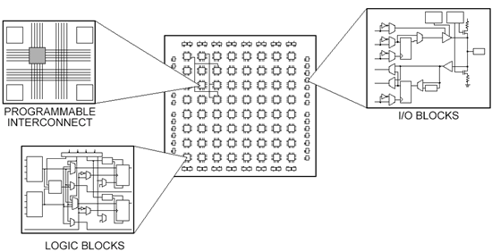
3. what is FPGA ?
Field Programmable Gate Array
FPGAs
are programmable semiconductor devices that are based around a matrix
of Configurable Logic Blocks (CLBs) connected through programmable
interconnects. As opposed to Application Specific Integrated Circuits (ASICs),
where the device is custom built for the particular design, FPGAs can
be programmed to the desired application or functionality requirements.
Although One-Time Programmable (OTP) FPGAs are available, the dominant
type are SRAM-based which can be reprogrammed as the design evolves.
FPGAs
allow designers to change their designs very late in the design cycle–
even after the end product has been manufactured and deployed in the
field. In addition, Xilinx FPGAs allow for field upgrades to be
completed remotely, eliminating the costs associated with re-designing
or manually updating electronic systems.

4.Why FPGA?
Unlike
processors, FPGAs use dedicated hardware for processing logic and do
not have an operating system. Because the processing paths are
parallel, different operations do not have to compete for the same
processing resources. That means speeds can be very fast, and multiple
control loops can run on a single FPGA device at different rates.
5.Steps to Program Xilinx FPGA
FPGA Design methodology
The generalized implementation flow diagram of the project is as follows.

FIGURE 1 : General Implementation Flow Diagram
Initially
the market research should be carried out which covers the previous
version of the design and the current requirements on the design. Based
on this survey, the specification and the architecture must be
identified. Then the RTL modeling can be carried out in Verilog or VHDL
or Schematic with respect to the identified architecture. Once the RTL
modeling is done, it should be simulated and verified for all the cases.
The functional verification should meet the intended architecture and
should pass all the test cases. Once the functional verification is
clear, the RTL model will be taken to the synthesis process. Three
operations will be carried out in the synthesis process such as
- Translate
- Map
- Place and Route
The
developed RTL model will be translated to the mathematical equation
format which will be in the understandable format of the tool. These
translated equations will be then mapped to the library that is, mapped
to the hardware. Once the mapping is done, the gates are placed and
routed. Before these processes, the constraints can be given in order to
optimize the design. Finally the BIT MAP file will be generated that
has the design information in the binary format which will be dumped in
the FPGA board.
Schematic Design Entry
The
Xilinx Integrated Software Environment (ISE) allows users to design
circuits for Xilinx FPGA’s and CPLD’s. It involves the use of Project
Navigator, a user interface that helps user to manage the entire design
process including design entry, simulation, synthesis, implementation
and finally downloading the design onto FPGA or CPLD.
1. Start ISE from the Start menu by selecting Start -> Programs -> Xilinx ISE 9.2 -> Project Navigator. The ISE Project Navigator opens. The Project Navigator manages the sources and processes in ISE project.
2. The next step is to create a new ISE project. To create a new project for this tutorial:
- Select File -> New Project. The New Project Wizard appears as shown in Figure 2
- First, enter a location (directory path) for the new project.
- Type fadd (for example) in the Project Name field. After typing fadd in the Project Name field, a counter subdirectory is created automatically in the directory path selected.
- Select Schematic in the Top-Level Source Type list, indicating that the top-level file in project will be a schematic rather than HDL, EDIF or NGC/NGO. Click Next to go to the Device Properties window.

FIGURE 2 : Creating a new project
3. In the Device Properties window, select Target device, Simulator tool, Synthesis tool and Hardware language which is used to design code.
4. Click Next three times and reach the Project Summary window. This window gives an overview of project created so far. Click on Finish and the project is created. Verify that the project name is fadd.ise (shown
as the last component in the title bar of the Project Navigator). You
can also verify by going to the location where you created the project
and double-clicking on the folder named fadd.
5. Create a top level schematic for your design. In the Sources window, right click on
Xc3s400-4pq208 and select New Source. A New Source Wizard window appears as shown in Figure 3. Select Schematic and enter fadd under file name. Make sure the “Add to project” checkbox is checked.

FIGURE 3: Creation of a schematic source file
6. Click Next two times followed by Finish to create the fadd.sch file
under the project folder. Figure 4 shows the final layout of the
project after the source file is created. If the schematic is not
visible, click on the “fadd.sch” tab at the bottom of the main design
window to see the schematic.
- Select the required components from symbols by specifying proper category in source window.
- Drag and drop the component symbols.
- Assign ports and complete the circuit using wire.
- Check errors and warnings. Clearing those errors is must.
- Follow the standard procedure for simulation, synthesis and implementation

FIGURE 4: Project Navigator showing top-level schematic
Floorplanning
Floorplanning is the process of:
- Choosing the best grouping and connectivity of logic in a design, and
- Manually placing blocks of logic in an FPGA device.
The goals of floorplanning are to:
- Increase density, routability, or performance.
- Reduce route delays for selected logic by suggesting a better placement.
Floorplanning
has become necessary as designers create ever-more complex designs for
ever-larger FPGA devices. Implementation software has improved to meet
these complexities. On some designs, you can guide the implementation
software by means of a floorplan to:
- Higher system clock frequency
- Shorter implementation run times
- Greater consistency in timing
- In some cases, all of these benefits together
Benefits of Floorplanning
A good floorplan can:
- Improve performance.
- Enable a placed and routed design to meet timing.
Xilinx recommends floorplanning when a design:
- Does not meet timing consistently, or
- Has never met timing.
When to Floorplan
When to floorplan varies greatly among design teams. Design teams may floorplan:
- Before the first iteration through place and route.
- When a problem is identified before floorplanning.
- When a design does not consistently meet the setup timing constraint.
Floorplanning Considerations
- Floorplanning is often an iterative process. The first pass at a floorplan may address issues in one section of the design, only to reveal that a different section is failing.
- Floorplanning can hurt timing as well as improve it.
This is especially true when it is not clear what needs to be floor planned, and where the design needs to be placed.
- Multiple trials and notes about the design can help you create a working floorplan.
Floorplanner
The
Floorplanner is a graphical placement tool that gives you control over
placing a design into a target FPGA using a “drag and drop” paradigm
with the mouse pointer.
The
Floorplanner displays a hierarchical representation of the design in
the Design Hierarchy window using hierarchy structure lines and colors
to distinguish the different hierarchical levels. The Floorplan window
displays the floorplan of the target device into which you place logic
from the hierarchy. The following figure shows the windows on the PC
version.

FIGURE 5: Floorplanner Window
Floorplanning Prerequisites
The
Floorplanner is specifically intended to assist those users who require
some degree of handcrafting for their designs. You must understand both
the details of the device architectures and how floorplanning can be
used to refine a design. Successful floorplanning is very much an
iterative process and it can take time to develop a floorplan that
outperforms an "automatically" processed design. Because of the nature
of the Floor planner’s interaction with the automatic MAP and PAR tools,
several prerequisites are necessary in order to floorplan your design
successfully.
Detailed knowledge of the specifics of the target architecture and part
- Detailed knowledge of the specifics of the design being implemented
- A design that lends itself to floorplanning
- A willingness to iterate a floorplan to achieve the desired results
Features of the Floorplanner
The Floorplanner provides an easy-to-use graphical interface that offers the following features.
- Interacts at a high level of the design hierarchy, as well as with low-level elements such as I/Os, function generators, tristate buffers, flip-flops, and RAM/ROM
- Captures and imposes complex patterns, which is useful for repetitive logic structures such as interleaved buses
- Automatically distributes logic into columns or rows
- Uses dynamic rubber banding to show the rats nest connections
- Finds logic or nets by name or connectivity
- Permits design hierarchy rearrangement to simplify floorplanning
- Groups logic by connectivity or function
- Identifies placement problems in the Floorplan window
- Provides online help
No comments:
Post a Comment